
High-Frequency
Ultrasound Inspection Platform
OHLABS · High-Frequency Ultrasound NDT
Seeing what optical inspection cannot, OHLABS reveals hidden defects inside semiconductors, batteries, and industrial materials with high-frequency ultrasound scanning.
High-Frequency
Ultrasound Inspection Platform
Non-Destructive
Internal Defect Visualization
Sub-surface
Void · Crack · Delamination
Automation Ready
From Lab Analysis to In-line Systems
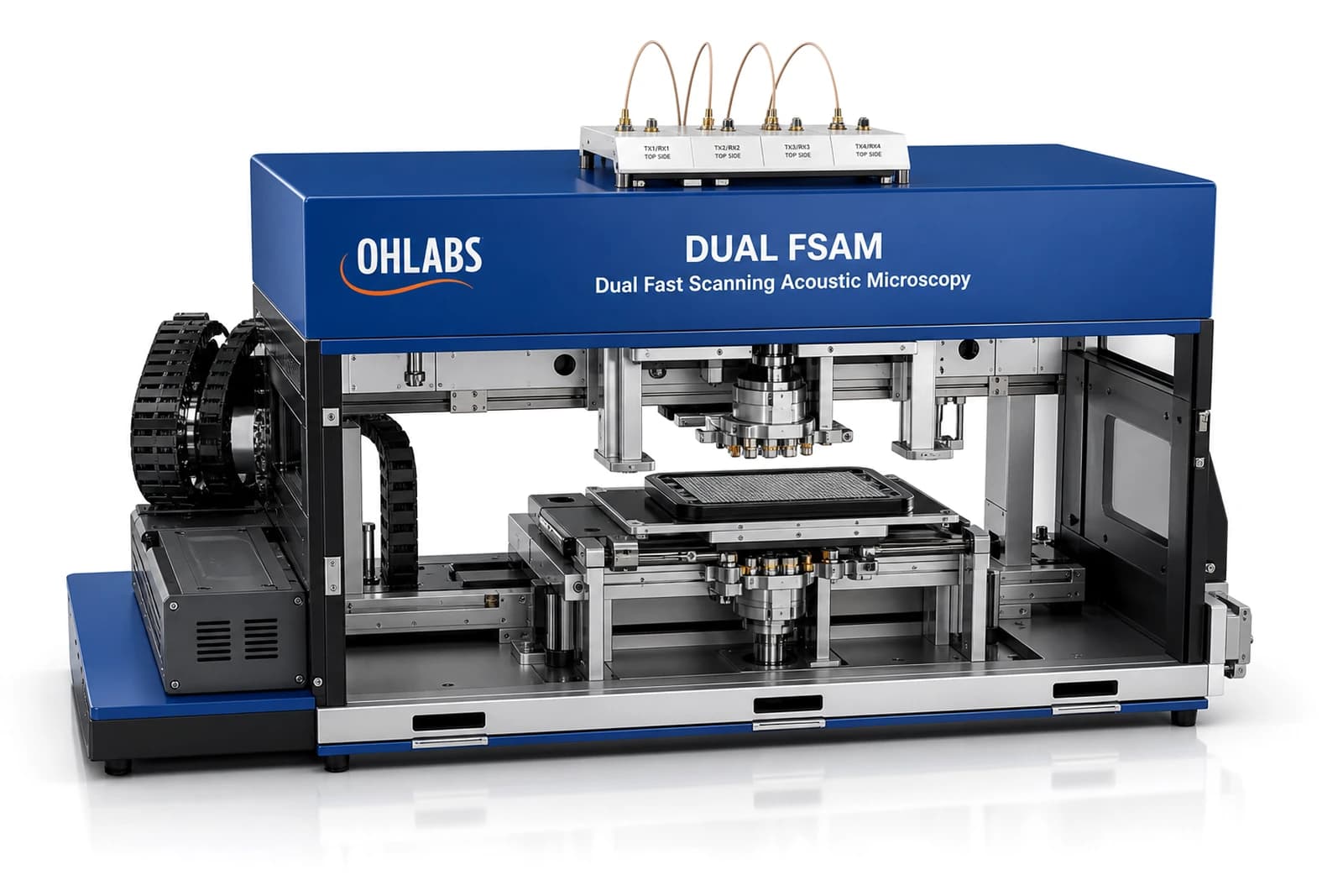
Dual FSAM
The carrier moves from the load bay into the scan stage, where top and bottom acoustic heads align through the sample and stream inspection data to the result panel.
Controlled transfer from load bay to stage
Top and bottom transducers scan left-right over the stopped sample
Live C-scan pulse and defect signal loop
Technology
OHLABS should be understood as a technical inspection company: acoustic hardware, scanning architecture, laser ultrasound direction, and software analysis working together.
Core acoustic inspection technology for visualizing internal defects without cutting, polishing, or damaging the sample.
Fast scanning acoustic microscopy architecture designed for advanced packaging, wafer, and precision material inspection.
Laser-based ultrasound inspection concept for contact-sensitive samples and advanced research workflows.
Software-assisted image review for classifying defect patterns and turning scan images into actionable engineering evidence.
Applications
The site leads with HBM and advanced packaging, then expands into batteries, power devices, MEMS, composites, and industrial inspection.
Internal inspection for stacked packages, bonding interfaces, and hidden voids in advanced semiconductor packaging.
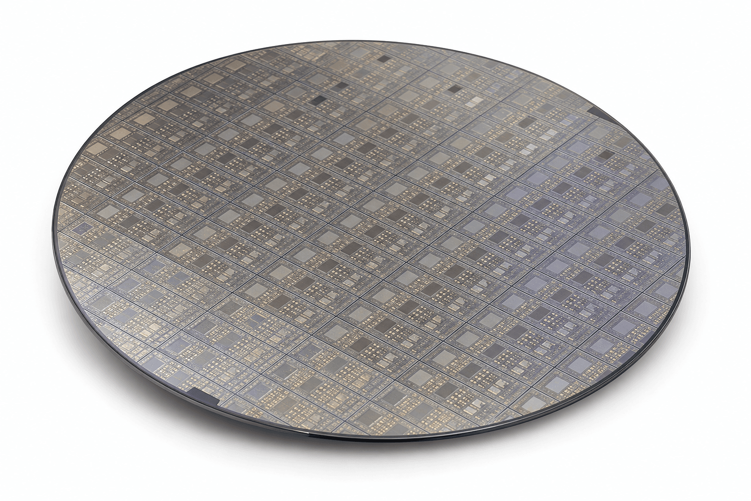
Wafer-level acoustic imaging for internal defects that optical inspection cannot expose.

Inspection support for modules where bonding quality and thermal reliability matter.
Validation & Resources
The strongest sales material is direct evidence: what optical inspection misses, what ultrasound reveals, and how each defect type appears in scan data.
Resource
Side-by-side evidence showing why internal defects require acoustic inspection instead of surface-only review.
Resource
A practical visual library for void, crack, delamination, and bonding anomaly patterns.
Resource
A buyer-friendly report structure for scan conditions, images, findings, and next inspection recommendations.
Resource
A future hub for datasheets, catalog PDFs, application notes, and scan request guides.

Company
OHLABS commercializes high-frequency ultrasound non-destructive inspection technology from Pukyong National University NBMLAB into practical systems for global engineering teams.
Sample Scan Request
Share your material, target defect, and inspection requirements. OHLABS will recommend a practical scan path before equipment discussions begin.